
The Knight Campus Graduate Internship Program's Semiconductor Track is hosting a Fall 2026 Hands-On Semiconductor Training Workshop — open to community college students, community college STEM faculty, and high school STEM teachers — no prior semiconductor experience required.
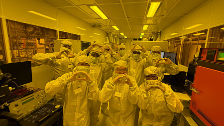
Participants will spend a full day, 9:00 a.m. to 4:00 p.m. on Sunday, November 8, inside the Phil and Penny Knight Campus for Accelerating Scientific Impact, stepping into an active cleanroom to see firsthand how atom-by-atom engineering turns raw materials into the chips powering everything from smartphones to AI. Past participants have called the experience "amazing," pointing to photolithography demonstrations and behind-the-scenes lab access as highlights.
The workshop pays: $275 for student participants and $800 for educators, with lodging and mileage potentially covered for those traveling more than 50 miles. To qualify, applicants must be U.S. citizens or permanent residents, at least 18 years old, and currently enrolled at a community college or working as a community college instructor or high school STEM teacher (students need at least one completed STEM course with a C or better).
Applications are due Monday, October 5, with selected participants notified on a rolling basis starting October 12. Register here.
The workshop is made possible by a $1.5 million award from Oregon's Higher Education Coordinating Commission. Questions can be directed to Allison Fujinaga at afujinag@uoregon.edu.